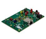
ADRV9009-W/PCBZ
Analog Devices Inc.
The ADRV9009 is a highly integrated, radio frequency (RF), agile transceiver offering dual transmitters and receivers, integrated synthesizers, and digital signal processing functions. The IC delivers a versatile combination of high performance and low power consumption demanded by 3G, 4G, and 5G macro cell time division duplex (TDD) base station applications.The receive path consists of two independent, wide bandwidth, direct conversion receivers with state-of-the-art dynamic range. The device also supports a wide bandwidth, time shared observation path receiver (ORx) for use in TDD applications. The complete receive subsystem includes automatic and manual attenuation control, dc offset correction, quadrature error correction (QEC), and digital filtering, thus eliminating the need?for these functions in the digital baseband. Several auxiliary functions, such as analog-to-digital converters (ADCs), digital-to-analog converters (DACs), and general-purpose inputs/outputs (GPIOs) for the power amplifier (PA), and RF front-end control are also integrated.In addition to automatic gain control (AGC), the ADRV9009 also features flexible external gain control modes, allowing significant flexibility in setting system level gain dynamically.The received signals are digitized with a set of four high dynamic range, continuous time ?-? ADCs that provide inherent antialiasing. The combination of the direct conversion architecture, which does not suffer from out of band image mixing, and the lack of aliasing, relaxes the requirements of the RF filters when compared to traditional intermediate frequency (IF) receivers.The transmitters use an innovative direct conversion modulator that achieves high modulation accuracy with exceptionally low noise.The observation receiver path consists of a wide bandwidth, direct conversion receiver with state-of-the-art dynamic range.The fully integrated phase-locked loop (PLL) provides high performance, low power, fractional-N RF frequency synthesis for the transmitter (Tx) and receiver (Rx) signal paths. An additional synthesizer generates the clocks needed for the converters, digital circuits, and the serial interface. A multichip synchronization mechanism synchronizes the phase of the RF local oscillator (LO) and baseband clocks between multiple ADRV9009 chips. Precautions are taken to provide the isolation required in high performance base station applications. All voltage controlled oscillators (VCOs) and loop filter components are integrated.The high speed JESD204B interface supports up to 12.288 Gbps lane rates, resulting in two lanes per transmitter and a single lane per receiver in the widest bandwidth mode. The interface also supports interleaved mode for lower bandwidths, thus reducing the total number of high speed data interface lanes to one. Both fixed and floating point data formats are supported. The floating point format allows internal AGC to be invisible to the demodulator device.The core of the ADRV9009 can be powered directly from 1.3 V regulators and 1.8 V regulators, and is controlled via a standard 4-wire serial port. Comprehensive power-down modes are included to minimize power consumption in normal use. The ADRV9009 is packaged in a 12 mm ? 12 mm, 196-ball chip scale ball grid array (CSP_BGA).Applications 3G, 4G, and 5G TDD macrocell base stations TDD active antenna systems Massive multiple input, multiple output (MIMO) Phased array radar Electronic warfare Military communications Portable test equipment
Distributor | SKU | Stock | MOQ | 1 | 10 | 50 | 100 | 1,000 | 10,000 |
---|---|---|---|---|---|---|---|---|---|
DigiKey | ADRV9009-W/PCBZ-ND | 4 | $2,094.52 | $2,094.52 | $2,094.52 | $2,094.52 | $2,094.52 | $2,094.52 | |
Analog Devices Inc | ADRV9009-W/PCBZ | 0 | $2,010.74 | $2,010.74 | $2,010.74 | $2,010.74 | $2,010.74 | $2,010.74 | |
element14 APAC | ADRV9009-W/PCBZ | 1 | 1 | * $2,115.62 | * $2,115.62 | * $2,115.62 | * $2,115.62 | * $2,115.62 | * $2,115.62 |
Farnell | ADRV9009-W/PCBZ | 2 | 1 | * $1,961.09 | * $1,961.09 | * $1,961.09 | * $1,961.09 | * $1,961.09 | * $1,961.09 |
Mouser Electronics | 584-ADRV9009-W/PCBZ | 9 | 1 | $2,167.64 | $2,167.64 | $2,167.64 | $2,167.64 | $2,167.64 | $2,167.64 |
Newark | ADRV9009-W/PCBZ | 1 | 1 | $2,100.74 | $2,100.74 | $2,100.74 | $2,100.74 | $2,100.74 | $2,100.74 |
Win Source | ADRV9009-W/PCBZ | 1 | 1 |
ADRV9029-LB/PCBZ
Analog Devices Inc.
The ADRV9029 is a highly integrated, radio frequency (RF) agile transceiver offering four independently controlled transmitters, dedicated observation receiver inputs for monitoring each transmitter channel, four independently controlled receivers, integrated synthesizers, and digital signal processing functions providing a complete transceiver solution. The device provides the performance demanded by cellular infrastructure applications, such as small cell base station radios, macro 3G/4G/5G systems, and massive multiple in/multiple out (MIMO) base stations.The receiver subsystem consists of four independent, wide bandwidth, direct conversion receivers with wide dynamic range. The four independent transmitters use a direct conversion modulator resulting in low noise operation with low power consumption. The device also includes two wide bandwidth, time shared, observation path receivers with two inputs each for monitoring transmitter outputs.The complete transceiver subsystem includes automatic and manual attenuation control, dc offset correction, quadrature error correction (QEC), and digital filtering, eliminating the need for these functions in the digital baseband. Other auxiliary functions such as analog-to-digital converters (ADCs), digital-to-analog converters (DACs), and general-purpose input/ outputs (GPIOs) that provide an array of digital control options are also integrated.To achieve a high level of RF performance, the transceiver includes five fully integrated phase-locked loops (PLLs). Two PLLs provide low noise and low power fractional-N RF synthesis for the transmitter and receiver signal paths. A third fully integrated PLL supports an independent local oscillator (LO) mode for the observation receiver. The fourth PLL generates the clocks needed for the converters and digital circuits, and a fifth PLL provides the clock for the serial data interface.A multichip synchronization mechanism synchronizes the phase of all LOs and baseband clocks between multiple ADRV9029 chips. All voltage controlled oscillators (VCOs) and loop filter components are integrated and adjustable through the digital control interface.This device contains a fully integrated, low power digital predistortion (DPD) adaptation engine for use in power amplifier linearization. DPD enables use of high efficiency power amplifiers, reducing the power consumption of base station radios while also reducing the number of SERDES lanes necessary to interface with baseband processors.The low power crest factor reduction (CFR) engine of the ADRV9029 reduces the peak to average ratio (PAR) of the input signal, enabling higher efficiency transmit line ups while reducing the processing load on baseband processors.The serial data interface consists of four serializer lanes and four deserializer lanes. The interface supports both the JESD204B and JESD204C standards, operating at data rates up to 24.33 Gbps. The interface also supports interleaved mode for lower bandwidths, thus reducing the number of high speed data interface lanes to one. Both fixed and floating-point data formats are supported. The floating-point format allows internal automatic gain control (AGC) to be invisible to the demodulator device.The ADRV9029 is powered directly from 1.0 V, 1.3 V, and 1.8 V regulators and is controlled via a standard serial peripheral interface (SPI) serial port. Comprehensive power-down modes are included to minimize power consumption in normal use. The ADRV9029 is packaged in a 14 mm ? 14 mm, 289-ball chip scale ball grid array (CSP_BGA).APPLICATIONS3G/4G/5G TDD and FDD massive MIMO, macro and small cell base stations
Distributor | SKU | Stock | MOQ | 1 | 10 | 50 | 100 | 1,000 | 10,000 |
---|---|---|---|---|---|---|---|---|---|
DigiKey | 505-ADRV9029-LB/PCBZ-ND | 8 | $3,050.78 | $3,050.78 | $3,050.78 | $3,050.78 | $3,050.78 | $3,050.78 | |
Mouser Electronics | 584-ADRV9029-LB/PCBZ | 2 | 1 | $3,288.83 | $3,288.83 | $3,288.83 | $3,288.83 | $3,288.83 | $3,288.83 |
Newark | ADRV9029-LB/PCBZ | 0 | 1 | $3,391.06 | $3,391.06 | $3,391.06 | $3,391.06 | $3,391.06 | $3,391.06 |
ADRV9029-MB/PCBZ
Analog Devices Inc.
The ADRV9029 is a highly integrated, radio frequency (RF) agile transceiver offering four independently controlled transmitters, dedicated observation receiver inputs for monitoring each transmitter channel, four independently controlled receivers, integrated synthesizers, and digital signal processing functions providing a complete transceiver solution. The device provides the performance demanded by cellular infrastructure applications, such as small cell base station radios, macro 3G/4G/5G systems, and massive multiple in/multiple out (MIMO) base stations.The receiver subsystem consists of four independent, wide bandwidth, direct conversion receivers with wide dynamic range. The four independent transmitters use a direct conversion modulator resulting in low noise operation with low power consumption. The device also includes two wide bandwidth, time shared, observation path receivers with two inputs each for monitoring transmitter outputs.The complete transceiver subsystem includes automatic and manual attenuation control, dc offset correction, quadrature error correction (QEC), and digital filtering, eliminating the need for these functions in the digital baseband. Other auxiliary functions such as analog-to-digital converters (ADCs), digital-to-analog converters (DACs), and general-purpose input/ outputs (GPIOs) that provide an array of digital control options are also integrated.To achieve a high level of RF performance, the transceiver includes five fully integrated phase-locked loops (PLLs). Two PLLs provide low noise and low power fractional-N RF synthesis for the transmitter and receiver signal paths. A third fully integrated PLL supports an independent local oscillator (LO) mode for the observation receiver. The fourth PLL generates the clocks needed for the converters and digital circuits, and a fifth PLL provides the clock for the serial data interface.A multichip synchronization mechanism synchronizes the phase of all LOs and baseband clocks between multiple ADRV9029 chips. All voltage controlled oscillators (VCOs) and loop filter components are integrated and adjustable through the digital control interface.This device contains a fully integrated, low power digital predistortion (DPD) adaptation engine for use in power amplifier linearization. DPD enables use of high efficiency power amplifiers, reducing the power consumption of base station radios while also reducing the number of SERDES lanes necessary to interface with baseband processors.The low power crest factor reduction (CFR) engine of the ADRV9029 reduces the peak to average ratio (PAR) of the input signal, enabling higher efficiency transmit line ups while reducing the processing load on baseband processors.The serial data interface consists of four serializer lanes and four deserializer lanes. The interface supports both the JESD204B and JESD204C standards, operating at data rates up to 24.33 Gbps. The interface also supports interleaved mode for lower bandwidths, thus reducing the number of high speed data interface lanes to one. Both fixed and floating-point data formats are supported. The floating-point format allows internal automatic gain control (AGC) to be invisible to the demodulator device.The ADRV9029 is powered directly from 1.0 V, 1.3 V, and 1.8 V regulators and is controlled via a standard serial peripheral interface (SPI) serial port. Comprehensive power-down modes are included to minimize power consumption in normal use. The ADRV9029 is packaged in a 14 mm ? 14 mm, 289-ball chip scale ball grid array (CSP_BGA).APPLICATIONS3G/4G/5G TDD and FDD massive MIMO, macro and small cell base stations
Distributor | SKU | Stock | MOQ | 1 | 10 | 50 | 100 | 1,000 | 10,000 |
---|---|---|---|---|---|---|---|---|---|
DigiKey | 505-ADRV9029-MB/PCBZ-ND | 1 | $3,050.78 | $3,050.78 | $3,050.78 | $3,050.78 | $3,050.78 | $3,050.78 | |
Mouser Electronics | 584-ADRV9029-MB/PCBZ | 4 | 1 | $3,288.83 | $3,288.83 | $3,288.83 | $3,288.83 | $3,288.83 | $3,288.83 |
Newark | ADRV9029-MB/PCBZ | 0 | 1 | $3,391.06 | $3,391.06 | $3,391.06 | $3,391.06 | $3,391.06 | $3,391.06 |
Win Source | ADRV9029-MB/PCBZ | 1 | 1 |
ADV3205-EVALZ
Analog Devices Inc.
The ADV3205 is a fully buffered crosspoint switch matrix that operates on ?5 V, making it ideal for video applications. It offers a ?3 dB signal bandwidth of 60 MHz and channel switch times of less than 60 ns with 0.1% settling. The ADV3205 has excellent crosstalk performance, and ground/power pins surround all inputs and outputs to provide extra shielding required for the most demanding applications. The differential gain and differential phase of better than 0.1% and 0.1?, respectively, along with 0.1 dB flatness out to 10 MHz, make the ADV3205 an excellent choice for many video applications.The ADV3205 includes 16 independent output buffers that can be placed into a disabled state for paralleling crosspoint outputs. The ADV3205 has a gain of +2 and operates on voltage supplies of ?5 V while consuming only 34 mA of current. Channel switching is performed via a serial digital control (which can accommodate daisy-chaining of several devices) or via a parallel control, allowing updating of an individual output without reprogramming the entire array.?The ADV3205 is packaged in a 100-lead LQFP and is available over the commercial temperature range of 0?C to 70?C.?ApplicationsCCTV surveillanceVideo routers (NTSC, PAL, S-Video, SECAM)Video conferencing
Distributor | SKU | Stock | MOQ | 1 | 10 | 50 | 100 | 1,000 | 10,000 |
---|---|---|---|---|---|---|---|---|---|
element14 APAC | ADV3205-EVALZ | 0 | 1 | * $695.05 | * $695.05 | * $695.05 | * $695.05 | * $695.05 | * $695.05 |
Farnell | ADV3205-EVALZ | 0 | 1 | * $477.00 | * $477.00 | * $477.00 | * $477.00 | * $477.00 | * $477.00 |
Mouser Electronics | N/A | 0 |
ADV3220-EVALZ
Analog Devices Inc.
The ADV3219 and ADV3220 are high speed, high slew rate,buffered, 2:1 analog multiplexers. They offer a ?3 dB signalbandwidth greater than 800 MHz and channel switch times ofless than 20 ns with 1% settling. With ?82 dB of crosstalk and?88 dB isolation (at 5 MHz), the ADV3219 and ADV3220 areuseful in many high speed applications. The differential gain ofless than 0.02% and the differential phase of less than 0.02?,together with 0.1 dB flatness beyond 100 MHz while driving a75 ? back terminated load, make the ADV3219 and ADV3220ideal for all types of signal switching. The ADV3219/ADV3220 include an output buffer that can beplaced into a high impedance state to allow multiple outputs tobe connected together for cascading stages without the off channelsloading the output bus. The ADV3219 has a gain of +1, and theADV3220 has a gain of +2; they both operate on ?5 V supplieswhile consuming less than 7.5 mA of idle current.The ADV3219/ADV3220 are available in the 8-lead LFCSPpackage over the extended industrial temperature range of?40?C to +85?C. Applications Routing of high speed signals including ??Video (NTSC, PAL, S, SECAM, YUV, and RGB) ??Compressed video (MPEG, wavelet) ??3-level digital video (HDB3) Data communications Telecommunications
Distributor | SKU | Stock | MOQ | 1 | 10 | 50 | 100 | 1,000 | 10,000 |
---|---|---|---|---|---|---|---|---|---|
Mouser Electronics | N/A | 0 |
ADV3227-EVALZ
Analog Devices Inc.
The ADV3226/ADV3227 are high speed 16 ? 16 analog crosspoint switch matrices. They offer a ?3 dB signal bandwidth greater than 750 MHz and channel switch times of less than 20 ns with 1% settling.The ADV3226/ADV3227 include 16 independent output buffers that can be placed into a high impedance state for paralleling crosspoint outputs to prevent off channels from loading the output bus. The ADV3226 has a gain of +1 and the ADV3227 has a gain of +2. They both operate on voltage supplies of ?5 V while consuming only 118 mA (ADV3226) and 133 mA (ADV3227) of idle current. Channel switching is performed via a serial digital control that can accommodate daisy chaining of several devices or via a parallel control to allow updating of an individual output without reprogramming the entire array.The ADV3226/ADV3227 are available in the 100-lead LFCSP package over the extended industrial temperature range of ?40?C to +85?C.Applications Routing of high speed signals including ? ? Video (NTSC, PAL, S, SECAM, YUV, RGB) ? ? Compressed video (MPEG, wavelet) ? ? 3-level digital video (HDB3) Data communications Telecommunications
Distributor | SKU | Stock | MOQ | 1 | 10 | 50 | 100 | 1,000 | 10,000 |
---|---|---|---|---|---|---|---|---|---|
Mouser Electronics | N/A | 0 |
ADV3228-EVALZ
Analog Devices Inc.
The ADV3228/ADV3229 are high speed 8 ? 8 analog crosspoint switch matrices. They offer a ?3 dB large signal bandwidth of 750 MHz (ADV3228) and a slew rate of 2500 V/?s.The ADV3228/ADV3229 include eight independent output buffers that can be placed into a high impedance state for paralleling crosspoint outputs to prevent off channels from loading the output bus. The ADV3228 has a gain of +1, the ADV3229 has a gain of +2, and they both operate on voltage supplies of ?5 V. Channel switching is performed via a serial digital control that can accommodate daisy chaining of several devices or via a parallel control to allow updating of an individual output without reprogramming the entire array.The ADV3228/ADV3229 are available in the 72-lead LFCSP package over the extended industrial temperature range of ?40?C to +85?C.Applications Routing of high speed signals including: ? ? ? Video (NTSC, PAL, S, SECAM, YUV, RGB) ? ? ? Compressed video (MPEG, wavelet) ? ? ? 3-level digital video (HDB3) Data communications Telecommunications
Distributor | SKU | Stock | MOQ | 1 | 10 | 50 | 100 | 1,000 | 10,000 |
---|---|---|---|---|---|---|---|---|---|
Mouser Electronics | N/A | 0 |
ADXL213EB
Analog Devices Inc.
The ADXL213 is a low cost, low power, complete dual axis accelerometer with signal conditioned, duty cycle modulated outputs, all on a single monolithic IC. The ADXL213 measures acceleration with a full-scale range of ?1.2 g (typical). The ADXL213 can measure both dynamic acceleration (e.g., vibration) and static acceleration (e.g., gravity).The outputs are digital signals whose duty cycles (ratio of pulse width to period) are proportional to acceleration (30%/g). The duty cycle outputs can be directly measured by a microcontroller without an A/D converter or glue logic.Innovative design techniques are used to ensure high zero g bias stability (typically better than 0.25 mg/?C), as well as tight sensitivity stability (typically better than 50 ppm/?C).The typical noise floor is 160 ?g/?, allowing signals below 1 mg (0.06? of inclination) to be resolved in tilt sensing applications using narrow bandwidths (The user selects the bandwidth of the accelerometer usingcapacitors CX and CYM at the XFILT and YFILT pins. Bandwidths of0.5 Hz to 250 Hz may be selected to suit the application.The ADXL213 is available in a 5mm x 5mm x 2mm, 8-pad hermetic LCC package.ApplicationsAutomotive tilt alarmData projectorsNavigationPlatform stabilization/levelingAlarms and motion detectorsHigh accuracy, 2-axis tilt sensing
Distributor | SKU | Stock | MOQ | 1 | 10 | 50 | 100 | 1,000 | 10,000 |
---|---|---|---|---|---|---|---|---|---|
DigiKey | ADXL213EB-ND | 4 | $52.50 | $52.50 | $52.50 | $52.50 | $52.50 | $52.50 | |
Analog Devices Inc | ADXL213EB | 0 | $46.56 | $46.56 | $46.56 | $46.56 | $46.56 | $46.56 | |
Arrow North American Components | ADXL213EB | 0 | 1 | $37.84 | $36.12 | $36.12 | $35.27 | $34.83 | $34.83 |
element14 APAC | ADXL213EB | 0 | 1 | * $42.03 | * $42.03 | * $42.03 | * $42.03 | * $42.03 | * $42.03 |
Farnell | ADXL213EB | 0 | 1 | * $34.58 | * $34.58 | * $34.58 | * $34.58 | * $34.58 | * $34.58 |
Mouser Electronics | 584-ADXL213EB | 2 | 1 | $53.01 | $53.01 | $53.01 | $53.01 | $53.01 | $53.01 |
Newark | ADXL213EB | 0 | $44.39 | $41.78 | $38.30 | $38.30 | $38.30 | $38.30 | |
Verical Marketplace | ADXL213EB | 23 | 1 | $47.27 | $40.29 | $39.20 | $39.20 | $39.20 | $39.20 |
Win Source | ADXL213EB | 720 | 1 |
Amplifier Mezzanine Card for ADA4500-2
Analog Devices Inc.
The Analog Devices, Inc., amplifier mezzanine card (AMC) analog-to-digital converter (ADC) driver evaluates the performance of amplifiers in 8-lead, single and dual SOIC, 6-lead single SOT23, 8-lead dual MSOP, and 16-lead LFCSP
packages. This add on board can be inserted on ADC evaluation boards using its 7-pin header. Figure 1 shows the AMC mounted on an Analog Devices, Inc., ADC evaluation board.
The AMC can support any of Analog Devices operational amplifiers and ADC drivers in different packages. The user can configure the ADC driver as a Sallen-Key low-pass, high-pass, or band-pass filter, as a multiple feedback low-pass, high-pass, or band-pass filter, or as an inverting and noninverting operational amplifier. The user can also configure the AMC to drive a single-ended, fully differential, or a single-ended signal to a differential ADC.
Optimized power and ground planes ensure low noise and high speed operation. Component placement and power supply bypassing are optimized for maximum circuit flexibility and performance. The AMC evaluation board accepts 0402 or 0603 surface mount technology (SMT) components, 1206 bypass capacitors, and 2.54 mm headers.
All components are placed on the primary side. No components are placed on the secondary side.
Distributor | SKU | Stock | MOQ | 1 | 10 | 50 | 100 | 1,000 | 10,000 |
---|---|---|---|---|---|---|---|---|---|
DigiKey | AMC-ADA4500-2ARMZ-ND | 1 | $36.45 | $36.45 | $36.45 | $36.45 | $36.45 | $36.45 | |
Analog Devices Inc | AMC-ADA4500-2ARMZ | 0 | $35.31 | $35.31 | $35.31 | $35.31 | $35.31 | $35.31 | |
Mouser Electronics | 584-AMCADA45002ARMZ | 0 | 1 | $36.54 | $36.54 | $36.54 | $36.54 | $36.54 | $36.54 |
Amplifier Mezzanine Card for ADA4805-2
Analog Devices Inc.
The Analog Devices, Inc., amplifier mezzanine card (AMC) analog-to-digital converter (ADC) driver evaluates the performance of amplifiers in 8-lead, single and dual SOIC, 6-lead single SOT23, 8-lead dual MSOP, and 16-lead LFCSP
packages. This add on board can be inserted on ADC evaluation boards using its 7-pin header. Figure 1 shows the AMC mounted on an Analog Devices, Inc., ADC evaluation board.
The AMC can support any of Analog Devices operational amplifiers and ADC drivers in different packages. The user can configure the ADC driver as a Sallen-Key low-pass, high-pass, or band-pass filter, as a multiple feedback low-pass, high-pass, or band-pass filter, or as an inverting and noninverting operational amplifier. The user can also configure the AMC to drive a single-ended, fully differential, or a single-ended signal to a differential ADC.
Optimized power and ground planes ensure low noise and high speed operation. Component placement and power supply bypassing are optimized for maximum circuit flexibility and performance. The AMC evaluation board accepts 0402 or 0603 surface mount technology (SMT) components, 1206 bypass capacitors, and 2.54 mm headers.
All components are placed on the primary side. No components are placed on the secondary side.
Distributor | SKU | Stock | MOQ | 1 | 10 | 50 | 100 | 1,000 | 10,000 |
---|---|---|---|---|---|---|---|---|---|
DigiKey | 505-AMC-ADA4805-2ARMZ-ND | 1 | $33.48 | $33.48 | $33.48 | $33.48 | $33.48 | $33.48 | |
Analog Devices Inc | AMC-ADA4805-2ARMZ | 0 | $32.36 | $32.36 | $32.36 | $32.36 | $32.36 | $32.36 | |
Mouser Electronics | 584-AMCADA48052ARMZ | 0 | 1 | $33.49 | $33.49 | $33.49 | $33.49 | $33.49 | $33.49 |