|
|

Texas Instruments
TPS5430DDA
|

Texas Instruments
TPS5450DDA
|
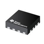
Texas Instruments
TS3A44159RSVR
|
Texas Instruments
TUSB3200ACPAH
|
Texas Instruments
UC1845W
|
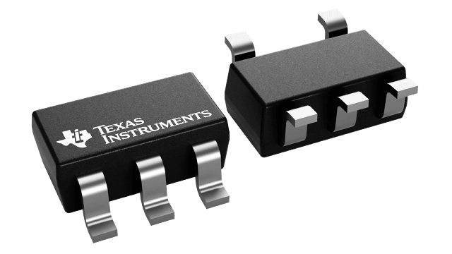
Texas Instruments
SN74LVC1G32DBVR
|

Texas Instruments
SN74LVC1G332DCKR
|

Texas Instruments
SN74LVC1G38DCKR
|
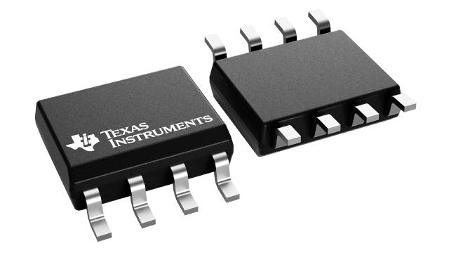
Texas Instruments
NE5532AP
|

Texas Instruments
NE5532P
|
| Price |
|
$3.58 |
|
|
|
|
|
|
|
|
$0.77 |
| RoHS |
|
Compliant |
Compliant |
Compliant |
Compliant |
Not Compliant |
Compliant |
Yes |
Yes |
Compliant |
Yes |
| Lead Status |
|
No |
No |
No |
No |
No |
No |
Yes |
Yes |
No |
Yes |
| Vout(Max)(V) |
|
31 |
31 |
|
|
|
|
|
|
|
|
| Rating |
|
Catalog |
Catalog |
Catalog |
|
Military |
Catalog |
Catalog |
Catalog |
Catalog |
Catalog |
| Switching Frequency(Max)(kHz) |
|
500 |
500 |
|
|
|
|
|
|
|
|
| Duty Cycle(Max)(%) |
|
87 |
89 |
|
|
50 |
|
|
|
|
|
| Operating Temperature Range(C) |
|
-40 to 125 |
-40 to 125 |
-40 to 85 |
|
-55 to 125 |
-40 to 125,-40 to 85 |
-40 to 125,-40 to 85 |
-40 to 125,-40 to 85 |
0 to 70 |
0 to 70 |
| Vout(Min)(V) |
|
1.23 |
1.22 |
|
|
|
|
|
|
|
|
| Vin(Max)(V) |
|
36 |
36 |
|
|
30 |
|
|
|
|
|
| Type |
|
Converter |
Converter |
|
|
|
|
|
|
|
|
| Regulated Outputs(#) |
|
1 |
1 |
|
|
|
|
|
|
|
|
| Control Mode |
|
Voltage Mode |
Voltage Mode |
|
|
|
|
|
|
|
|
| Special Features |
|
Enable |
Enable |
|
|
Error Amplifier,Multi-topology |
Ioff,down translation to Vcc,low power |
Ioff,down translation to Vcc,low power |
Ioff,down translation to Vcc,low power |
|
|
| Switching Frequency(Min)(kHz) |
|
500 |
500 |
|
|
|
|
|
|
|
|
| Iq(Typ)(mA) |
|
3 |
3 |
|
|
|
|
|
|
|
|
| Package Group |
|
SO PowerPAD |
SO PowerPAD |
QFN,TSSOP,UQFN |
|
CDIP,CFP,LCCC |
DSBGA,SC70,SON,SOT,SOT-23,X2SON |
SC70,SON,SOT,SOT-23,DSBGA |
DSBGA,SC70,SON,SOT-23 |
PDIP,SO,SOIC |
PDIP,SO,SOIC |
| Approx. Price (US$) |
|
1.85 | 1ku |
2.00 | 1ku |
0.35 | 1ku |
|
|
0.06 | 1ku |
0.06 | 1ku |
0.07 | 1ku |
0.33 | 1ku |
0.26 | 1ku |
| Iout(Max)(A) |
|
3 |
5 |
|
|
|
|
|
|
|
|
| Vin(Min)(V) |
|
5.5 |
5.5 |
|
|
7.6 |
|
|
|
|
|
| Charge Injection(Max)(pC) |
|
|
|
109 |
|
|
|
|
|
|
|
| Input/Ouput Voltage(Max)(V) |
|
|
|
4.3 |
|
|
|
|
|
|
|
| Turn off Time (Disable)(ns) |
|
|
|
50 |
|
|
|
|
|
|
|
| Input/Output OFF-state Capacitance(Typ)(pF) |
|
|
|
51 |
|
|
|
|
|
|
|
| Additional Features |
|
|
|
Break-before-make,Low Harmonic Distortion,Low Power |
|
|
|
|
|
N/A |
N/A |
| Digital input leakage(Max)(uA) |
|
|
|
0.05 |
|
|
|
|
|
|
|
| Configuration |
|
|
|
1 |
|
|
|
|
|
|
|
| Ron(Max)(Ohms) |
|
|
|
0.8 |
|
|
|
|
|
|
|
| Input/Output ON-state Capacitance(Typ)(pF) |
|
|
|
162 |
|
|
|
|
|
|
|
| ON-state leakage current(Max)(A) |
|
|
|
0.05 |
|
|
|
|
|
|
|
| VCC(Max)(V) |
|
|
|
4.3 |
|
|
5.5 |
5.5 |
5.5 |
|
|
| ICC(Max)(uA) |
|
|
|
0.7 |
|
|
|
|
|
|
|
| VIH(Min)(V) |
|
|
|
1 |
|
|
|
|
|
|
|
| Mux Configuration |
|
|
|
1 |
|
|
|
|
|
|
|
| Ron(Typ)(Ohms) |
|
|
|
0.37 |
|
|
|
|
|
|
|
| Input/Ouput Voltage(Min)(V) |
|
|
|
0 |
|
|
|
|
|
|
|
| Ron Channel Match(Max)() |
|
|
|
0.1 |
|
|
|
|
|
|
|
| Number of Channels(#) |
|
|
|
4 |
|
|
|
|
|
2 |
2 |
| Package Size |
|
|
|
mm2 |
|
mm2 |
mm2 |
mm2 |
mm2 |
mm2 |
mm2 |
| THD(Typ)(%) |
|
|
|
0.003 |
|
|
|
|
|
|
|
| Crosstalk(dB) |
|
|
|
-73 |
|
|
|
|
|
|
|
| Off Isolation(Typ)(dB) |
|
|
|
-71 |
|
|
|
|
|
|
|
| OFF-state leakage current(Max)(A) |
|
|
|
0.05 |
|
|
|
|
|
|
|
| Input/Output Continuous Current(Max)(mA) |
|
|
|
200 |
|
|
|
|
|
|
|
| VCC(Min)(V) |
|
|
|
1.65 |
|
|
1.65 |
1.65 |
1.65 |
|
|
| VIL(Max)(V) |
|
|
|
0.6 |
|
|
|
|
|
|
|
| ESD HBM(kV) |
|
|
|
2 |
|
|
|
|
|
|
|
| THD(Typ)(dB) |
|
|
|
-90.46 |
|
|
|
|
|
|
|
| ESD Charged Device Model(kV) |
|
|
|
1 |
|
|
|
|
|
|
|
| RON Flatness(Max)(Ohms) |
|
|
|
0.8 |
|
|
|
|
|
|
|
| Bandwidth(Max)(MHz) |
|
|
|
35 |
|
|
|
|
|
|
|
| Bandwidth(MHz) |
|
|
|
35 |
|
|
|
|
|
|
|
| Turn on Time (Enable)(Max)(ns) |
|
|
|
75 |
|
|
|
|
|
|
|
| UVLO Thresholds On/Off(V) |
|
|
|
|
|
8.4/7.6 |
|
|
|
|
|
| Frequency(Max)(kHz) |
|
|
|
|
|
500 |
|
|
|
|
|
| Topology |
|
|
|
|
|
Boost,Flyback,Forward |
|
|
|
|
|
| Control Method |
|
|
|
|
|
Current |
|
|
|
|
|
| 3-State Output |
|
|
|
|
|
|
No |
No |
No |
|
|
| Voltage(Nom)(V) |
|
|
|
|
|
|
1.8,2.5,3.3,5 |
1.8,2.5,3.3,5 |
1.8,2.5,3.3,5 |
|
|
| Technology Family |
|
|
|
|
|
|
LVC |
LVC |
LVC |
|
|
| tpd @ Nom Voltage(Max)(ns) |
|
|
|
|
|
|
7.2,4.4,3.6,3.4 |
17.2,6.2,4.8,3.5 |
10,6,4.5,3.9 |
|
|
| Output Drive (IOL/IOH)(Max)(mA) |
|
|
|
|
|
|
32/-32 |
32/-32 |
32/-32 |
|
|
| Logic |
|
|
|
|
|
|
True |
True |
True |
|
|
| Schmitt Trigger |
|
|
|
|
|
|
No |
No |
No |
|
|
| Gate Type |
|
|
|
|
|
|
OR |
OR |
NAND |
|
|
| Bits(#) |
|
|
|
|
|
|
1 |
1 |
1 |
|
|
| Sub-Family |
|
|
|
|
|
|
OR Gate |
OR Gate |
NAND Gate |
|
|
| ICC @ Nom Voltage(Max)(mA) |
|
|
|
|
|
|
0.01 |
0.01 |
0.01 |
|
|
| F @ Nom Voltage(Max)(Mhz) |
|
|
|
|
|
|
150 |
150 |
150 |
|
|
| Output Type |
|
|
|
|
|
|
|
CMOS |
CMOS |
|
|
| Input Type |
|
|
|
|
|
|
|
CMOS/TTL |
CMOS/TTL |
|
|
| Architecture |
|
|
|
|
|
|
|
|
|
Bipolar |
Bipolar |
| Iq per channel(Typ)(mA) |
|
|
|
|
|
|
|
|
|
4 |
4 |
| Total Supply Voltage(Max)(+5V=5, +/-5V=10) |
|
|
|
|
|
|
|
|
|
30 |
30 |
| Slew Rate(Typ)(V/us) |
|
|
|
|
|
|
|
|
|
9 |
9 |
| GBW(Typ)(MHz) |
|
|
|
|
|
|
|
|
|
10 |
10 |
| Vos (Offset Voltage @ 25C)(Max)(mV) |
|
|
|
|
|
|
|
|
|
4 |
4 |
| Offset Drift(Typ)(uV/C) |
|
|
|
|
|
|
|
|
|
0 |
0 |
| Output Current(Typ)(mA) |
|
|
|
|
|
|
|
|
|
38 |
38 |
| CMRR(Min)(dB) |
|
|
|
|
|
|
|
|
|
70 |
70 |
| Total Supply Voltage(Min)(+5V=5, +/-5V=10) |
|
|
|
|
|
|
|
|
|
10 |
10 |
| Input Bias Current(Max)(pA) |
|
|
|
|
|
|
|
|
|
800000 |
800000 |
| Vn at 1kHz(Typ)(nV/rtHz) |
|
|
|
|
|
|
|
|
|
5 |
5 |
| CMRR(Typ)(dB) |
|
|
|
|
|
|
|
|
|
100 |
100 |
| Iq per channel(Max)(mA) |
|
|
|
|
|
|
|
|
|
8 |
8 |
| Rail-to-Rail |
|
|
|
|
|
|
|
|
|
No |
No |