
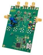
ADN4605-EVALZ
Analog Devices Inc.
X-Stream 4.25 Gbps 40 40 Digital Crosspoint Switch Features: DC to 4.25 Gbps per port NRZ data rate Adjustable receive equalization 3 dB, 6 dB, or 12 dB boost Compensates over 40 inches of FR4 at 4.25 Gbps Adjustable transmit preemphasis/deemphasis Programmable boost and output level Compensates over 40 inches of FR4 at 4.25 Gbps Low Power 105 mW per channel at 2.5 V (400 mVP-P differential output level swing) 40 × 40, fully differential, nonblocking array Double rank connection programming with dual maps Low jitter, typically <25 ps Flexible 2.5 V to 3.3 V supply range DC- or ac-coupled differential PECL/CML inputs Differential CML outputs Per-lane polarity inversion for routing ease 50 Ω on-chip I/O termination with disable feature Supports 8b10b, scrambled or uncoded NRZ data Serial (I2C slave or SPI) control interface Parallel control interface
| Distributor | SKU | Stock | MOQ | 1 | 10 | 50 | 100 | 1,000 | 10,000 |
|---|---|---|---|---|---|---|---|---|---|
| DigiKey | ADN4605-EVALZ | 1 | 1 | $945.95 | $945.95 | $945.95 | $945.95 | $945.95 | $945.95 |
| Analog Devices Inc | ADN4605-EVALZ | 0 | $866.70 | $866.70 | $866.70 | $866.70 | $866.70 | $866.70 | |
| Arrow North American Components | ADN4605-EVALZ | 0 | 1 | $817.64 | $817.64 | $817.64 | $817.64 | $817.64 | $817.64 |
| Mouser Electronics | ADN4605-EVALZ | 4 | 1 | $938.99 | $938.99 | $938.99 | $938.99 | $938.99 | $938.99 |
| Verical Marketplace | ADN4605-EVALZ | 1 | 1 | $950.56 | $950.56 | $950.56 | $950.56 | $950.56 | $950.56 |
| Distributor | SKU | Stock | MOQ | 1 | 10 | 50 | 100 | 1,000 | 10,000 |
|---|---|---|---|---|---|---|---|---|---|
| DigiKey | ADL5336-EVALZ-ND | 1 | 1 | $167.54 | $167.54 | $167.54 | $167.54 | $167.54 | $167.54 |
| Arrow North American Components | ADL5336-EVALZ | 0 | 1 | ||||||
| element14 APAC | ADL5336-EVALZ | 0 | 1 | * $205.91 | * $205.91 | * $205.91 | * $205.91 | * $205.91 | * $205.91 |
| Farnell | ADL5336-EVALZ | 0 | 1 | * $170.49 | * $170.49 | * $170.49 | * $170.49 | * $170.49 | * $170.49 |
| Mouser Electronics | 584-ADL5336-EVALZ | 0 | 1 | ||||||
| Newark | ADL5336-EVALZ | 0 | $168.75 | $168.75 | $168.75 | $168.75 | $168.75 | $168.75 |

| Distributor | SKU | Stock | MOQ | 1 | 10 | 50 | 100 | 1,000 | 10,000 |
|---|---|---|---|---|---|---|---|---|---|
| DigiKey | AD8231-EVALZ | 1 | 1 | $71.92 | $71.92 | $71.92 | $71.92 | $71.92 | $71.92 |
| Analog Devices Inc | AD8231-EVALZ | 0 | $63.99 | $63.99 | $63.99 | $63.99 | $63.99 | $63.99 | |
| Arrow Europe | AD8231-EVALZ | 1 | 1 | $58.21 | $58.21 | $58.21 | $58.21 | $58.21 | $58.21 |
| Arrow North American Components | AD8231-EVALZ | 0 | 1 | $60.32 | $60.32 | $60.32 | $60.32 | $60.32 | $60.32 |
| element14 APAC | AD8231-EVALZ | 1 | 1 | $89.19 | $89.19 | $89.19 | $89.19 | $89.19 | $89.19 |
| Farnell | AD8231-EVALZ | 1 | 1 | $52.03 | $52.03 | $52.03 | $52.03 | $52.03 | $52.03 |
| Mouser Electronics | AD8231-EVALZ | 26 | 1 | $66.55 | $66.55 | $66.55 | $66.55 | $66.55 | $66.55 |
| Newark | AD8231-EVALZ | 1 | 1 | $69.10 | $69.10 | $69.10 | $69.10 | $69.10 | $69.10 |
| Verical Marketplace | AD8231-EVALZ | 2 | 1 | $67.41 | $0.00 | $0.00 | $0.00 | $0.00 | $0.00 |
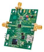
ADL5811-EVALZ
Analog Devices Inc.
High IP3, 700 MHz to 2800 MHz, Double Balanced, Passive Mixer, IF Amplifier, and Wideband LO Amplifier
| Distributor | SKU | Stock | MOQ | 1 | 10 | 50 | 100 | 1,000 | 10,000 |
|---|---|---|---|---|---|---|---|---|---|
| DigiKey | ADL5811-EVALZ-ND | 0 | |||||||
| Mouser Electronics | 584-ADL5811-EVALZ | 0 | 1 |

AD7280ABSTZ-RL
Analog Devices Inc.
Lithium Ion Battery Monitoring System Features: 12-bit ADC, 1 μs per channel conversion time 6 analog input channels, CM range 0.5 V to 27.5 V 6 auxiliary ADC Inputs ±1.6 mV cell voltage accuracy On-chip voltage regulator Cell balancing interface Daisy-chain interface Internal reference: ±3 ppm/°C 1.8 μA power-down current High input impedance Serial interface with alert function See data sheet for additional features
| Distributor | SKU | Stock | MOQ | 1 | 10 | 50 | 100 | 1,000 | 10,000 |
|---|---|---|---|---|---|---|---|---|---|
| DigiKey | AD7280ABSTZ-RL | 0 | 2000 | $8.79 | |||||
| Analog Devices Inc | AD7280ABSTZ-RL | 0 | |||||||
| Arrow North American Components | AD7280ABSTZ-RL | 0 | 2000 | $7.45 | |||||
| Mouser Electronics | AD7280ABSTZ-RL | 0 | 2000 | $7.79 | |||||
| Verical Marketplace | AD7280ABSTZ-RL | 14000 | 2000 | $7.90 |

| Distributor | SKU | Stock | MOQ | 1 | 10 | 50 | 100 | 1,000 | 10,000 |
|---|---|---|---|---|---|---|---|---|---|
| DigiKey | AD6641-500EBZ-ND | 1 | 1 | $416.22 | $262.13 | $250.06 | $250.06 | $216.08 | $216.08 |
| Mouser Electronics | N/A | 0 |

ADP1874
Analog Devices Inc.
Synchronous Buck Controller with Constant On-Time and Valley Current Mode
| Distributor | SKU | Stock | MOQ | 1 | 10 | 50 | 100 | 1,000 | 10,000 |
|---|---|---|---|---|---|---|---|---|---|
| DigiKey | ADP1874-1.0-EVALZ-ND | 1 | 1 | $78.29 | $3.35 | $3.08 | $2.79 | $2.57 | $2.48 |
| Mouser Electronics | N/A | 0 |
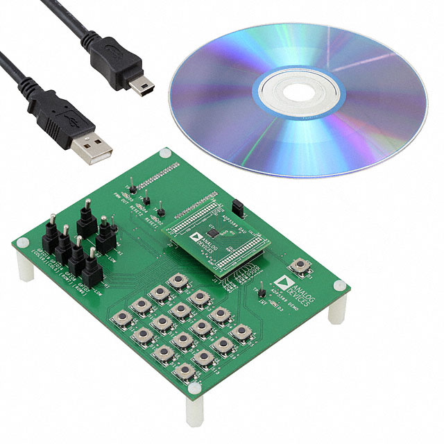
| Distributor | SKU | Stock | MOQ | 1 | 10 | 50 | 100 | 1,000 | 10,000 |
|---|---|---|---|---|---|---|---|---|---|
| DigiKey | ADP5589CP-EVALZ-ND | 0 | 1 | $197.11 | $197.11 | $197.11 | $197.11 | $197.11 | $197.11 |
| element14 APAC | ADP5589CP-EVALZ | 0 | 1 | * $295.55 | * $295.55 | * $295.55 | * $295.55 | * $295.55 | * $295.55 |
| Farnell | ADP5589CP-EVALZ | 0 | 1 | * $224.67 | * $224.67 | * $224.67 | * $224.67 | * $224.67 | * $224.67 |
| Mouser Electronics | 584-ADP5589CP-EVALZ | 0 | 1 | ||||||
| Newark | ADP5589CP-EVALZ | 0 | $200.00 | $200.00 | $200.00 | $200.00 | $200.00 | $200.00 | |
| Win Source | ADP5589CP-EVALZ | 529 | 1 |

AD820BRZ-REEL7
Analog Devices Inc.
Single-Supply, Rail-to-Rail, Low Power FET-Input Op Amp Features: True single-supply operation Output swings rail-to-rail Input voltage range extends below ground Single-supply capability from 5 V to 36 V Dual-supply capability from ±2.5 V to ±18 V Excellent load drive Capacitive load drive up to 350 pF Minimum output current of 15 mA Excellent ac performance for low power 800 μA maximum quiescent current Unity-gain bandwidth: 1.8 MHz Slew rate of 3 V/μs Excellent dc performance 800 μV maximum input offset voltage 2 μV/°C typical offset voltage drift 25 pA maximum input bias current Low noise: 13 nV/√Hz @ 10 kHz
| Distributor | SKU | Stock | MOQ | 1 | 10 | 50 | 100 | 1,000 | 10,000 |
|---|---|---|---|---|---|---|---|---|---|
| DigiKey | AD820BRZ-REEL7 | 760 | 1 | $14.32 | $11.30 | $10.54 | $9.71 | $8.96 | $8.96 |
| Analog Devices Inc | AD820BRZ-REEL7 | 0 | $10.44 | $9.44 | $9.00 | $7.81 | $7.46 | $7.46 | |
| Arrow North American Components | AD820BRZ-REEL7 | 0 | 750 | $7.93 | $7.93 | ||||
| element14 APAC | AD820BRZ-REEL7 | 703 | 10 | * $12.49 | * $11.66 | * $10.75 | * $10.52 | * $10.52 | |
| Farnell | AD820BRZ-REEL7 | 753 | 10 | * $11.60 | * $10.83 | * $10.27 | * $9.19 | * $9.19 | |
| Mouser Electronics | AD820BRZ-REEL7 | 2377 | 1 | $12.19 | $8.60 | $7.61 | $6.46 | $6.43 | $6.43 |
| Newark | AD820BRZ-REEL7 | 3 | 1 | $14.33 | $11.30 | $10.27 | $9.99 | $9.99 | $9.99 |
| Verical Marketplace | AD820BRZ-REEL7 | 66 | 1 | $10.77 | $9.09 | $8.65 | $0.00 | $6.15 | $6.15 |
| Win Source | AD820BRZ-REEL7 | 1660 | 4 | $11.79 | $8.16 | $8.16 | $8.16 | $8.16 |
AD8572
Analog Devices Inc.
Zero-Drift, Single-Supply, Rail-to-Rail Input/Output Operational Amplifiers
| Distributor | SKU | Stock | MOQ | 1 | 10 | 50 | 100 | 1,000 | 10,000 |
|---|---|---|---|---|---|---|---|---|---|
| DigiKey | AD8572ARUZ-REELCT-ND | 3852 | 1 | $6.84 | $5.27 | $4.88 | $4.45 | $4.01 | $3.34 |
| Mouser Electronics | N/A | 0 |