|
|

Texas Instruments
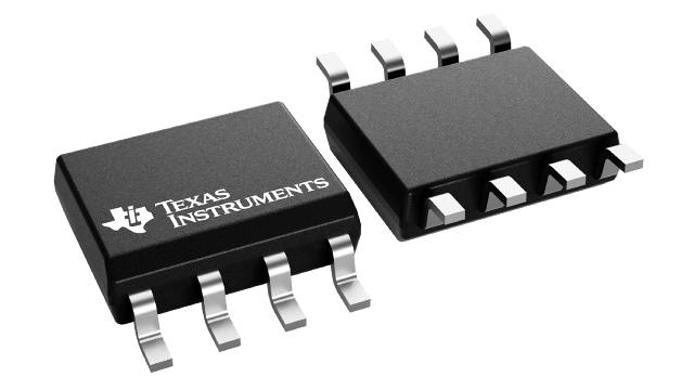
OPA2992IDR
|

Texas Instruments
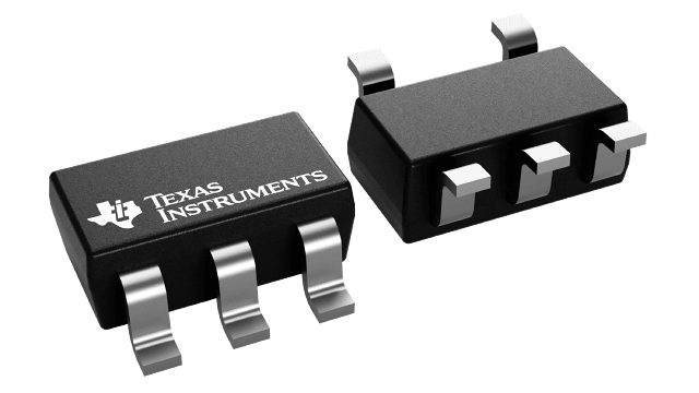
OPA387DBVT
|

Texas Instruments
AFE7900IABJ
|

Texas Instruments
INA186A5IYFDR
|

Texas Instruments
OPA210IDBVR
|

Texas Instruments
TUSB217AIRWBR
|

Texas Instruments
TPS3899DL30DSER
|

Texas Instruments
AMC1202DWVR
|

Texas Instruments
TLV7044QPWRQ1
|

Texas Instruments
TPS628692ARQYR
|
| Price |
|
|
|
|
|
|
|
|
|
|
|
| RoHS |
|
Y |
Y |
Y |
Y |
Y |
Y |
Y |
Y |
Y |
Y |
| Lead Status |
|
Y |
Y |
Y |
Y |
Y |
Y |
Y |
Y |
Y |
Y |
| Architecture |
|
CMOS |
CMOS |
Pipeline |
|
Bipolar |
|
|
|
|
|
| CMRR(typ)(dB) |
|
115 |
150 |
|
|
140 |
|
|
|
|
|
| Features |
|
EMI Hardened,MUX Friendly,Small Size |
Zero Drift |
High-performance,Input buffer |
Bidirectional,High precision,Low-side Capable |
Super Beta |
USB 2.0 Redriver with 5 Meter Cable Redriving Strength with CDP+DCP |
Detection time delay,Reset time delay,Separate VDD & sense,Undervoltage monitor only |
|
Fail-safe,Hysteresis,POR |
Adaptive/Dynamic Voltage Scaling,Enable,Forced PWM,I2C/PMBus,Light load efficiency,Output discharge,Over Current Protection,Power good,Soft Start Fixed,Synchronous Rectification,UVLO fixed,VID Interface |
| GBW(typ)(MHz) |
|
10.6 |
5.7 |
|
|
18 |
|
|
|
|
|
| Input common mode headroom (to negative supply)(typ)(V) |
|
0 |
-0.2 |
|
|
1.5 |
|
|
|
|
|
| Input common mode headroom (to positive supply)(typ)(V) |
|
0 |
0.1 |
|
|
-1.5 |
|
|
|
|
|
| Iout(typ)(A) |
|
0.065 |
0.055 |
|
|
0.065 |
|
|
|
|
|
| Iq per channel(typ)(mA) |
|
2.4 |
0.57 |
|
|
2.2 |
|
|
|
0.000315 |
|
| Number of channels |
|
2 |
1 |
|
1 |
1 |
1 |
|
|
4 |
|
| Offset drift(typ)(V/C) |
|
0.25 |
0.003 |
|
|
0.1 |
|
|
|
|
|
| Operating temperature range(C) |
|
-40 |
-40 |
-40 |
-40 |
-40 |
-40 |
-40 |
-40 to 125 |
-40 |
-40 |
| Output swing headroom (to negative supply)(typ)(V) |
|
0.048 |
0.001 |
|
|
0.2 |
|
|
|
|
|
| Output swing headroom (to positive supply)(typ)(V) |
|
-0.048 |
-0.001 |
|
|
-0.2 |
|
|
|
|
|
| Package area(mm^2) |
|
29.4 |
8.12 |
289 |
|
8.12 |
2.56 |
2.25 |
|
32 |
3.75 |
| Package size (L x W)(mm) |
|
4.9 x 6 |
2.9 x 2.8 |
17 x 17 |
1.4000000000000001 x 1 |
2.9 x 2.8 |
1.6 x 1.6 |
1.5 x 1.5 |
|
5 x 6.4 |
2.5 x 1.5 |
| Package type |
|
SOIC |
SOT-23 |
FCBGA |
DSBGA |
SOT-23 |
X2QFN |
WSON |
|
TSSOP |
VQFN-HR |
| Pin count |
|
8.0 |
5.0 |
400 |
|
5.0 |
12.0 |
6.0 |
|
14.0 |
9.0 |
| Rail-to-rail |
|
In,Out |
In,Out |
|
|
Out |
|
|
|
In |
|
| Rating |
|
Catalog |
Catalog |
Catalog |
Catalog |
Catalog |
Catalog |
Catalog |
Catalog |
Automotive |
Catalog |
| Slew rate(typ)(V/s) |
|
32 |
2.8 |
|
|
6.4 |
|
|
|
|
|
| TI functional safety category |
|
|
|
|
|
|
|
Functional Safety-Capable |
|
|
|
| TI package name |
|
D |
DBV |
|
|
DBV |
|
|
|
|
|
| Total supply voltage (+5 V = 5, 5 V = 10)(max)(V) |
|
40 |
5.5 |
|
|
36 |
|
|
|
|
|
| Total supply voltage (+5 V = 5, 5 V = 10)(min)(V) |
|
2.7 |
1.7 |
|
|
4.5 |
|
|
|
|
|
| Vn at 1 kHz(typ)(nVHz) |
|
7 |
8.5 |
|
|
2.2 |
|
|
|
|
|
| Vos (offset voltage at 25C)(max)(mV) |
|
1 |
0.002 |
|
|
0.035 |
|
|
|
8 |
|
| TI.com inventory |
|
2672 |
72001 |
905 |
74080 |
92163 |
77829 |
10706 |
0 |
121571 |
27328 |
| Approx. price(US$) |
|
.74 | 1ku |
1.188 | 1ku |
1198 | 1ku |
.42 | 1ku |
1.155 | 1ku |
2.381 | 1ku |
.398 | 1ku |
2.65 | 1ku |
.655 | 1ku |
.9 | 1ku |
| Input bias current(max)(pA) |
|
|
150 |
|
|
2000 |
|
|
|
|
|
| THD + N at 1 kHz(typ)(%) |
|
|
0.002 |
|
|
0.000025 |
|
|
|
|
|
| Analog input BW(MHz) |
|
|
|
7400 |
|
|
|
|
|
|
|
| Applications |
|
|
|
General purpose |
|
|
|
|
|
|
|
| Input buffer |
|
|
|
Yes |
|
|
|
|
|
|
|
| Interface type |
|
|
|
JESD204B,JESD204C |
|
|
|
|
|
|
|
| Interpolation |
|
|
|
10x,12x,15x,16x,18x,20x,24x,30x,32x,36x,3x,4.5x,40x,48x,4x,60x,64x,6x,7.5x,72x,80x,8x,96x,9x |
|
|
|
|
|
|
|
| Number of DAC channels |
|
|
|
4 |
|
|
|
|
|
|
|
| Number of DDCs per RX |
|
|
|
2 |
|
|
|
|
|
|
|
| Number of DUCs per TX |
|
|
|
2 |
|
|
|
|
|
|
|
| Number of TXs and RXs |
|
|
|
4 TX, 6 RX |
|
|
|
|
|
|
|
| Number of input channels |
|
|
|
6 |
|
|
|
|
|
|
|
| Power consumption(typ)(mW) |
|
|
|
6359 |
|
|
|
|
|
|
|
| RF frequency(max)(MHz) |
|
|
|
7400 |
|
|
|
|
|
|
|
| RF frequency(min)(MHz) |
|
|
|
5 |
|
|
|
|
|
|
|
| Resolution(Bits) |
|
|
|
14 |
|
|
|
|
|
|
|
| SFDR(dB) |
|
|
|
80 |
|
|
|
|
|
|
|
| Sample rate(max)(Msps) |
|
|
|
3000 |
|
|
|
|
|
|
|
| Sample/update rate(Msps) |
|
|
|
12000 |
|
|
|
|
|
|
|
| Bandwidth(kHz) |
|
|
|
|
27 |
|
|
|
|
|
|
| CMRR(min)(dB) |
|
|
|
|
120 |
|
|
|
|
|
|
| Common-mode voltage(max)(V) |
|
|
|
|
40 |
|
|
|
|
|
|
| Common-mode voltage(min)(V) |
|
|
|
|
-0.2 |
|
|
|
|
|
|
| Comparators(#) |
|
|
|
|
0 |
|
|
|
|
|
|
| Gain error drift ()(max)(ppm/C) |
|
|
|
|
10 |
|
|
|
|
|
|
| Gain error(%) |
|
|
|
|
1 |
|
|
|
|
|
|
| Input offset ()(max)(V) |
|
|
|
|
50 |
|
|
|
|
|
|
| Input offset drift ()(typ)(V/C) |
|
|
|
|
0.05 |
|
|
|
|
|
|
| Iq(max)(mA) |
|
|
|
|
0.09 |
|
|
|
|
|
|
| Product type |
|
|
|
|
Analog output |
|
|
|
|
|
|
| Slew rate(V/s) |
|
|
|
|
0.3 |
|
|
|
|
|
|
| Supply voltage(max)(V) |
|
|
|
|
5.5 |
|
6.5 |
6 |
|
|
|
| Supply voltage(min)(V) |
|
|
|
|
1.7 |
|
2.3 |
0.85 |
|
|
|
| Voltage gain(V/V) |
|
|
|
|
500 |
|
|
|
|
|
|
| Configuration |
|
|
|
|
|
|
USB 2.0 Single-channel |
|
|
|
|
| ESD HBM(typ)(kV) |
|
|
|
|
|
|
2 |
|
|
|
|
| Function |
|
|
|
|
|
|
USB 2.0 |
|
|
|
|
| Input/output voltage(max)(V) |
|
|
|
|
|
|
3.6 |
|
|
|
|
| Input/output voltage(min)(V) |
|
|
|
|
|
|
0 |
|
|
|
|
| Supply current(max)(A) |
|
|
|
|
|
|
36000 |
|
|
|
|
| Type |
|
|
|
|
|
|
Redriver |
|
|
|
Converter |
| USB speed(MBits) |
|
|
|
|
|
|
480 |
|
|
|
|
| Iq(typ)(mA) |
|
|
|
|
|
|
|
0.000025 |
|
|
0.004 |
| Number of supplies monitored |
|
|
|
|
|
|
|
1 |
|
|
|
| Output driver type/reset output |
|
|
|
|
|
|
|
Active-low,Open-drain |
|
|
|
| Reset threshold accuracy(%) |
|
|
|
|
|
|
|
0.5 |
|
|
|
| Threshold voltage 1(typ)(V) |
|
|
|
|
|
|
|
3 |
|
|
|
| Time delay(ms) |
|
|
|
|
|
|
|
0.03,0.04,0.05,0.08,0.3,30,6.2,619 |
|
|
|
| Watchdog timer WDI(s) |
|
|
|
|
|
|
|
None |
|
|
|
| Package Group |
|
|
|
|
|
|
|
|
SOIC|8 |
|
|
| Gain error drift (+/-)(Typ)(ppm/C) |
|
|
|
|
|
|
|
|
3 |
|
|
| CMTI(Min)(kV/s) |
|
|
|
|
|
|
|
|
100 |
|
|
| Input range(Vp-p) |
|
|
|
|
|
|
|
|
0.05 |
|
|
| Gain non-linearity (+/-)(Max)(%) |
|
|
|
|
|
|
|
|
0.03 |
|
|
| Isolation working voltage VIOWM (rms)(V) |
|
|
|
|
|
|
|
|
1000 |
|
|
| Isolation transient overvoltage VIOTM (peak)(V) |
|
|
|
|
|
|
|
|
4250 |
|
|
| Gain error (+/-)(Max)(%) |
|
|
|
|
|
|
|
|
0.2 |
|
|
| Small signal bandwidth(Typ)(kHz) |
|
|
|
|
|
|
|
|
280 |
|
|
| Package size |
|
|
|
|
|
|
|
|
mm2 |
|
|
| Input offset (+/-)(Max)(mV) |
|
|
|
|
|
|
|
|
0.05 |
|
|
| Input offset drift (+/-)(Typ)(uV/C) |
|
|
|
|
|
|
|
|
0.15 |
|
|
| Input bias current ()(max)(nA) |
|
|
|
|
|
|
|
|
|
0.002 |
|
| Output type |
|
|
|
|
|
|
|
|
|
Open-collector,Open-drain |
|
| Propagation delay time(s) |
|
|
|
|
|
|
|
|
|
3 |
|
| VICR(max)(V) |
|
|
|
|
|
|
|
|
|
6.6 |
|
| VICR(min)(V) |
|
|
|
|
|
|
|
|
|
0 |
|
| Vs(max)(V) |
|
|
|
|
|
|
|
|
|
6.5 |
|
| Vs(min)(V) |
|
|
|
|
|
|
|
|
|
1.6 |
|
| Control mode |
|
|
|
|
|
|
|
|
|
|
DCS-Control |
| DDR memory type |
|
|
|
|
|
|
|
|
|
|
LPDDR5 |
| Duty cycle(max)(%) |
|
|
|
|
|
|
|
|
|
|
100 |
| Iout(max)(A) |
|
|
|
|
|
|
|
|
|
|
6 |
| Maximum package height(mm) |
|
|
|
|
|
|
|
|
|
|
1.0 |
| Regulated outputs(#) |
|
|
|
|
|
|
|
|
|
|
1 |
| Switching frequency(max)(kHz) |
|
|
|
|
|
|
|
|
|
|
2400 |
| Switching frequency(min)(kHz) |
|
|
|
|
|
|
|
|
|
|
2400 |
| Vin(max)(V) |
|
|
|
|
|
|
|
|
|
|
5.5 |
| Vin(min)(V) |
|
|
|
|
|
|
|
|
|
|
2.4 |
| Vout(max)(V) |
|
|
|
|
|
|
|
|
|
|
3.35 |
| Vout(min)(V) |
|
|
|
|
|
|
|
|
|
|
0.8 |